Application design guide for SUPLET module power supply
time:02,08,2019
Using Module power supply, The user must design the corresponding peripheral application circuit .Some examples of typical application design are given below, The parameters and sample diagrams listed in the product specification
Contents
1、Test Configurations
2、Remote Sense
3、Input and Output Filter
4、Remote On/Off
5、Output Voltage Programming
6、Output Voltage Set-Point Adjustment
7、PMBus Addressing
8、Electromagnetic Compatibility (EMC)
9、Current Share
10、Reflow Soldering Information
11、Protection Features
12、Through-Hole Soldering Information
13、Considerations for Wave Soldering
1、Test Configurations
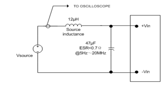
Figure1. Input Reflected Ripple Current Test Setup
Note: Measure input reflected ripple current with a simulated source inductance of 12μH. The measurement points for input reflected ripple current is showed above.
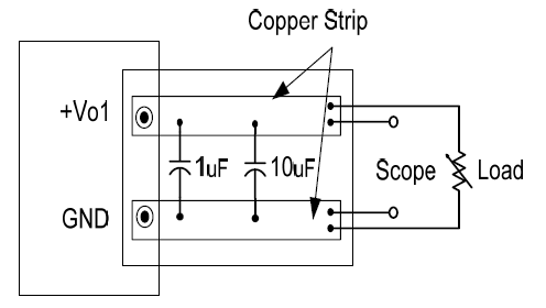
Figure2. Output Ripple and Noise Test Setup
Note: Scope measurements should be made using a BNC socket, with a 1μF ceramic capacitor and a 10 μF tantalum capacitor. Position the oscilloscope between 51mm and 76mm (2 inch and 3 inch) from the module.
2、Remote Sense
Remote sense minimizes the effects of distribution losses by regulating the voltage at the remote sense connections (see Figure 3). The voltage between the remote sense pins and the output terminals must not exceed the output voltage sense range (<10% Vo(nom)). The voltage between the +VO1 and GND terminals must not exceed the minimum output overvoltage protection value shown in the Electrical Specifications table. This limit includes any increase in voltage due to remote sense compensation and output voltage programming (trim). If not using the remote sense feature to regulate the output at the point of load, then connect +S to +VO1 and -S to GND. Although the output voltage can be increased by both the remote sense and by the trim, the maximum increase for the output voltage is not the sum of both. The maximum increase is the larger of either the remote sense or the trim. The amount of power delivered by the module is defined as the voltage at the output terminals multiplied by the output current. When using remote sense and trim, the output voltage of the module can be increased, at the same time output current would increase the power output of the module. Care should be taken to ensure that the maximum output power of the module remains at or below the maximum rated power.
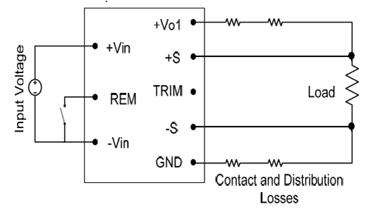
Figure3. Circuit Configuration for Remote Sense
3、Input and Output Filter
The BAA power module should be connected to a low acimpedance input source. A highly inductive source can affect the stability of the power module. An input capacitor must be placed directly adjacent to the input pin of the module, to minimize input ripple voltage and ensure module stability.
To reduce the output ripple and improve the dynamic response to a step load change, additional capacitor at the output can be used. For stable operation of the module, limit the capacitor to less than the maximum output capacitance as specified in the electrical specification table. Figure 4 shows the typical application circuit with input and output filters.
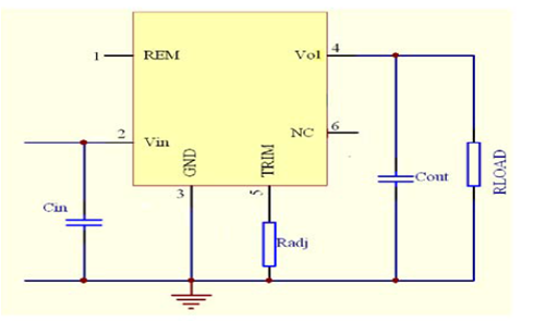
Figure 4. Typical application circuit
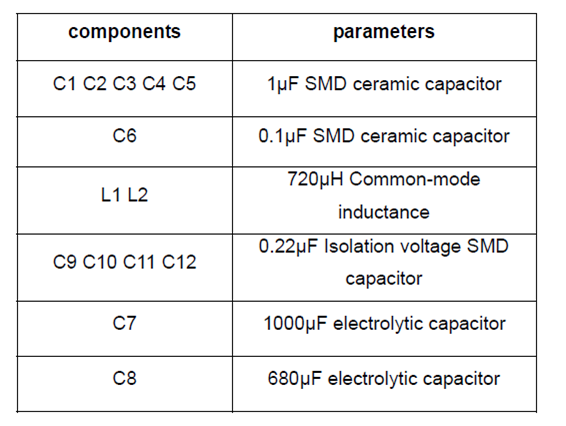
The power module should be connected to a low acimpedance input source. A highly inductive source can affect the stability of the power module. An input capacitor must be placed directly adjacent to the input pin of the module, to minimize input ripple voltage and ensure module stability. If you have more requirement of EMC, additional inductance is also needed. To reduce the output ripple and improve the dynamic response to a step load change, additional capacitor at the output can be used. For stable operation of the module, limit the capacitor to less than the maximum output capacitor as specified in the electrical specification table. Figure 4.1 shows the typical application circuit with input and output filters.
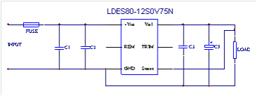
Figure 4.1 . Typical application circuit
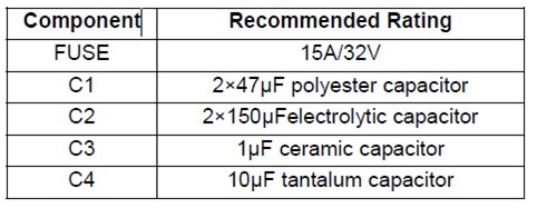
The Table below provides the recommended rating for usewith this family of products.
4、Remote On/Off
The REM pin is used to turn the power converter remote on or off via a system signal. This power module is negative logic version. When the REM pin is at logic low the power turns on and turns off at logic high. We also provide positive logic remote On/Off, turns the module on during logic high voltage and off during a logic low. To turn the power module on and off, the user must supply a switch to control the voltage between the REM pin and –Vin terminal (see Figure 5). A logic low is VREM = 0 to 1.5V.During logic high, the maximum VREM voltage generated by the power module is 20V. If not using the remote on/off feature, perform one of the following to turn the converter on: For negative logic, short REM pin to -Vin. For positive logic, leave REM pin open.
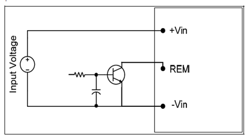
. Figure5. Remote On/Off Implementation
The BAA power modules feature an On/Off pin (REM) for remote On/Off control of the module. The remote On/Off operation is available by using a MOSFET, keeping the dissipation to a minimum. To turn the module on, the REM pin should be left open, and to turn the module off, the REM pin should be at 0~0.2Vdc.
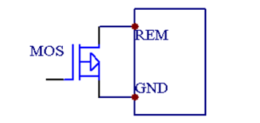
Figure 6. Remote On/Off Application Circuit
Two On/Off logic options are available. In the Positive Logic On/Off option, the module turns ON during a logic High on the On/Off pin and turns OFF during a logic Low. With the Negative Logic On/Off option, the module turns OFF during logic High and ON during logic Low. The On/Off signal should be always referenced to ground. For either On/Off logic option, leaving the On/Off pin disconnected will turn the module ON when input voltage is present.
For positive logic modules, the circuit configuration for using the On/Off pin is shown in Figure 7.
For negative logic On/Off modules, the circuit configuration is shown in Fig. 8.
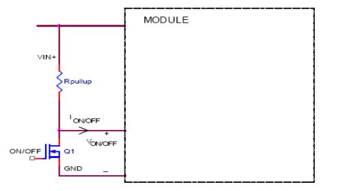
Figure 7. Circuit configuration for using positive On/Off logic.
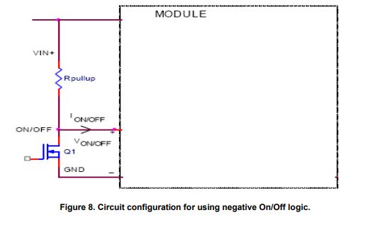
Figure 8. Circuit configuration for using negative On/Off logic.
5、Output Voltage Programming
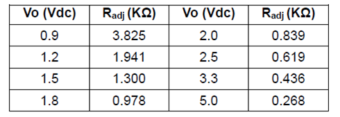
The output voltage of the module can be programmed to any voltage from 0.59Vdc to 5.1Vdc by connecting a single resistor Radj between the TRIM and GND pins (shown in Figure 9). Without an external resistor between the TRIM and ground, that is to say, the TRIM pin is left open, the output voltage is 0.59Vdc. To calculate the value of the resistor Radj for a particular output voltage Vo1, use thefollowing equation:

Where Vo = desired voltage.
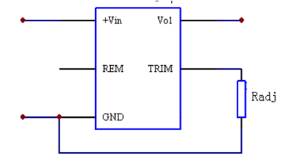
Figure 9. Output voltage programming application
The table below provides the Radj values required for somecommon output voltages:
6、Output Voltage Set-Point Adjustment
Output voltage trim allows the user to increase or decrease the output voltage set point of a module. This is accomplished by connecting an external resistor between the TRIM pin and either the +SENSE or -SENSE pins. The trim resistor should be positioned close to the module. If not using the trim feature, leave the TRIM pin open.
To increase the output voltage, refer to Figure 10. A trim resistor, Rtrimup, should be connected between the TRIM and +SENSE, with a value of:
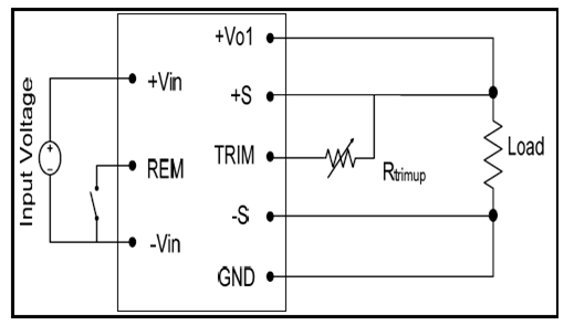
Figure10. Circuit Configuration to Increase Output Voltage.
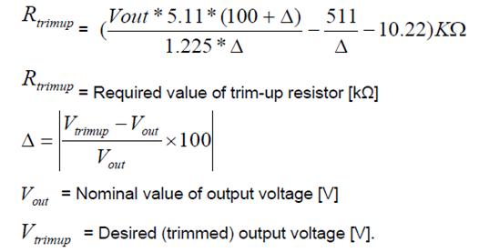
Trimming beyond 110% of the rated output voltage is not an acceptable design practice, as this condition could cause unwanted triggering of the output over-voltage protection (OVP) circuit .When trimming up, care must be taken not to exceed the converter’s maximum allowable output power.
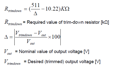
To decrease the output voltage (Figure.11), a trim resistor,Rtrimdown, should be connected between the TRIM and -SENSE, with a value of:
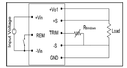
Figure11. Circuit Configuration to Decrease OutputVoltage.
7、PMBus Addressing
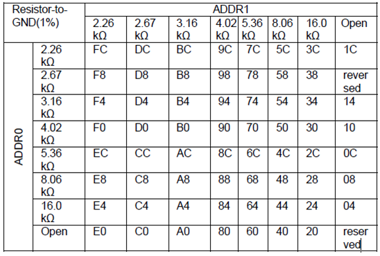
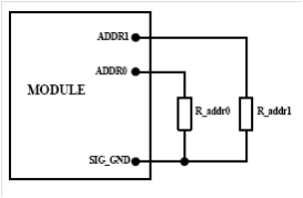
To properly set the device addresses, resistors with 1% tolerance must be connected from the ADDR0 and ADDR1 pins to ground. Once a valid PMBus address has been determined, communication with the controller can established via the PMBus bus of the controller.
Table 1: Device PMBus Address
8、Electromagnetic Compatibility (EMC)
The Figure 12 shows a suggested configuration to meet the conducted emission limits of EN55022 Class A.

Figure12. Recommended EMC application
The Figure 13 shows a suggested configuration to meet the conducted emission limits of EN55022 Class B.

Figure13. EMC testing typical application circuit
9、Current Share
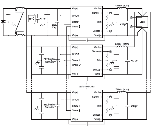
It shall connect units in parallel in order to increase output power and current for two or more units. Connect share 1 pins and share 2 pins of units in parallel. Don't disturb connecting cable. Connect output pins of units in parallel. It shall meet output impedance before connection. It shall ensure that each unit's power shall not exceed its rated output power and current shall not exceed its rated 95% of rated current in the parallel application.
10、Reflow Soldering Information
These power modules are large mass, low thermal resistance devices and typically heat up slower than other SMT components. It is recommended that the customer review data sheets in order to customize the solder reflow profile for each application board assembly. The following instructions must be observed when SMT soldering these units. Failure to observe these instructions may result in the failure of or cause damage to the modules, and can adversely affect long-term reliability. Typically, the eutectic solder melts at 217℃, wets the land, and subsequently wicks the device connection. Sufficient time must be allowed to fuse the plating on the connection to ensure a reliable solder joint. There are several types of SMT reflow technologies currently used in the industry. These surface mount power modules can be reliably soldered using natural forced convection, IR (radiantinfrared), or a combination of convection/IR. For reliable soldering the solder reflow profile should be established by accurately measuring the modules pin connector temperatures.
Lead-free (Pb-free) solder processes
For Pb-free solder processes, a pin temperature (TPIN) in excess of the solder melting temperature (TL, +217 to +221°C for Sn/Ag/Cu solder alloys) for more than 30 seconds, and a peak temperature of +235°C on all solder joints is recommended to ensure a reliable solder joint. For Pb-free solder processes, the product is qualified for MSL 3 according to IPC/JEDEC standard J-STD-020C. During reflow, TP must not exceed +245°C at any time.
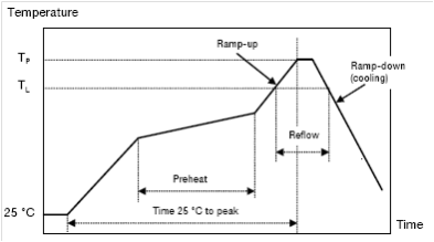
Figure14. Recommended reflow profile.
11、Protection Features
Over Current Protection
To provide protection in an output overload fault condition, the module is equipped with internal current limiting circuitry, and can endure current limiting continuously. At the point of current limit inception, the unit enters hiccup mode. The unit is configured with the auto-restart function, it will remain in the hiccup mode as long as the overcurrent condition exists, it operates normally once the output current is reduced back into its specified range.
Output Over Voltage Protection
The output overvoltage protection consists of circuitry that monitors the voltage on the output terminals. If the output voltage exceeds the overvoltage protection threshold, the module will operate in a hiccup mode until the overvoltage cause is cleared.
Over Temperature Protection
To provide protection under certain fault conditions, the module is equipped with a thermal shutdown circuit. The module will shutdown when the Tref temperature exceeds 115℃, but the thermal shutdown is not intended as a guarantee that the module will survive when the temperature beyond its rating. The module will automatically restarts after it cools down.
Input Under Voltage Lockout
Input undervoltage lockout is standard with this converter,when input voltages below the input undervoltage lockout limit, the module operation is disabled. It will only begin to operate once the input voltage is raised above the undervoltage lockout turn-on threshold.
Thermal Considerations
The power modules operate in a variety of thermal environments; however, sufficient cooling should be provided to help ensure reliable operation of the unit. Considerations include ambient temperature, airflow, module power dissipation, and the need for increased reliability. A reduction in the operating temperature of the module will result in an increase in reliability.
Heat Transfer Via Convection
Increasing airflow over the module enhances the heat transfer via convection. Derating figure showing the maximum output current that can be delivered by module versus local ambient temperature for natural convection.
12、Through-Hole Soldering Information
The product is intended for through-hole mounting in a PCB.When wave soldering is used, the temperature on the pins is specified to maximum 270 °C for maximum 10 seconds. Maximum preheat rate of 4°C/s and temperature of max 150 °C is suggested. When hands soldering care should be taken to avoid direct contact between the hot soldering iron tip and the pins for more than a few seconds in order to prevent overheating. A no-clean (NC) flux is recommended to avoid entrapment of cleaning fluids in cavities inside of the DC/DC power module. The residues may affect long time reliability and isolation voltage.
13、Considerations for Wave Soldering
For wave soldering, it is necessary to press the module with a test jig to avoid a gap exceeding 0.2mm between the module and the application board.

